Welcome to KingSong PCB Technology
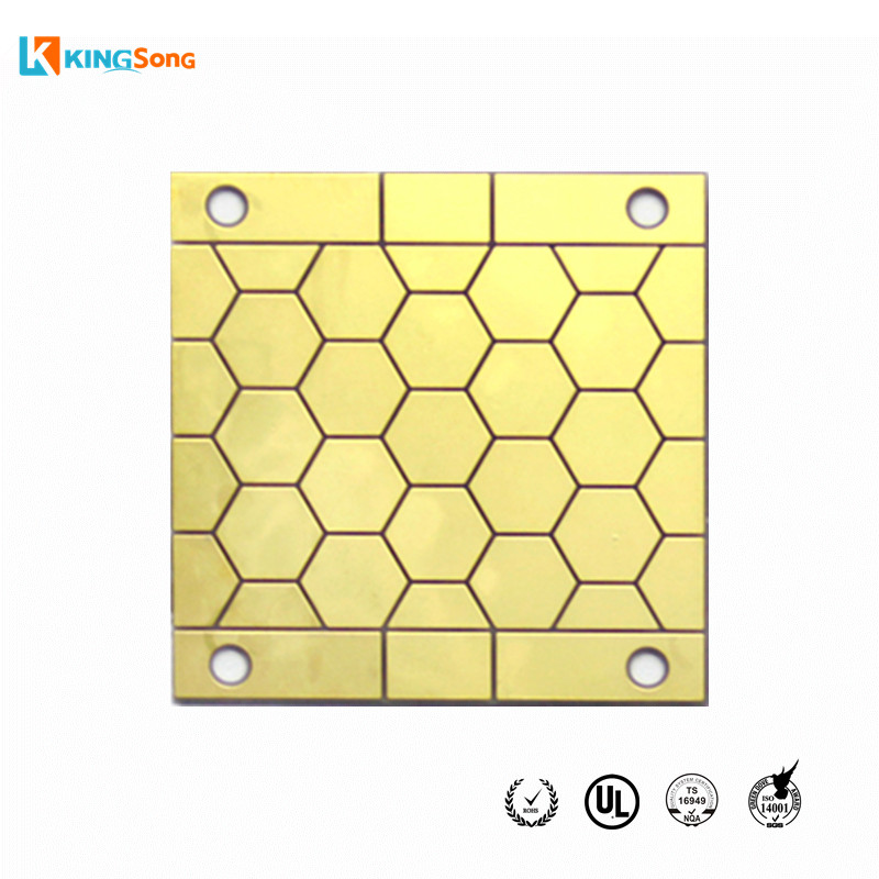
Image:LED Violet 0.635mm Aluminum Nitride Material Ceramic PCB

1.Ceramic PCB Board Capabilities:
Layer:1,2
Material:96% Alumina,99% Aluminium nitride(AIN),Sapphire,High Borosilicate Glass
Material Thickness(mm):0.38,0.635,0.5,1.0,1.2,1.5
Material Size(mm):120*120,127*127,132*132,140*130,190*140
Min Hole:0.075mm
Min Line width/space:0.1/0.1mm
Laser Outline: line width:0.1mm,tolerance:+/-0.1mm
Surface Finish:Immersion Silver,Immersion Gold,Immersion Tin,OSP
Copper Thickness(oz):H/H 1/1 2/2 3/3 4/4 5/5 6/6 7/7 8/8 9/9 10/10
Thermal conductivity value: 20~27W/m.K for Alumina; 180W~220W/m.K for Aluminium nitride , 27~30W/m.K for Sapphire,2 ~ 5 W/m.K for High Borosilicate Glass
Product Description:
At present, with the development of high efficiency, high density, and high power in the LED industry at home and abroad, it can be seen from 2017 to 2018, the overall domestic LED a rapid progress, is growing in power, the development of superior performance of heat dissipation material has become urgent to solve the problem of the LED heat dissipation.
For a long time, Al2O3 is the main substrate material of high power packaging.But the thermal conductivity of Al2O3 is low, and the thermal expansion coefficient does not match the chip material.Therefore, in terms of performance, cost and environmental protection, this substrate material cannot be the most ideal material for the development of high-power LED devices in the future.Aluminum nitride Material Ceramics PCB with high heat conductivity, high strength, high resistance rate, small density, low dielectric constant, non-toxic, will gradually replace traditional high-power LED substrate material, become one of the most promising future ceramic substrate materials,providing greater than 180W~220w/m.k,KingSong offers Ceramic printed circuit boards for your PCB needs.
Ceramic PCB Features:
Do not need to change the original processing procedures
Excellent mechanical strength
With good thermal conductivity
With resistance to erosion
Good surface characteristics, excellent flatness and flatness
Good thermal shock resistance
Low curl degree
Good stability under high temperature can be processed into a variety of complex shapes
Ceramic PCB Application:
high-accuracy clock oscillator,
voltage controlled oscillator (VCXO),
temperature compensated crystal oscillators (TCXOs),
oven controlled crystal oscillators (OCXOs);
emiconductor cooler;
electric power electronic control module;
high insulation & high pressure device;
high temperature (up to 800C)
high power LED
High Power semiconductor modules
solid state relay (SSR)
DC-DC module power sources
electric power transmitter modules
Solar-panel arrays
Intelligent power devices
Automotive electronics
High power semiconductor module
Solar panel components
Lighting industry
Aerospace
Communications
The power electronics industry
2.Delivery time:
Sample:3-5 or 12-15 working days,
Mass production:5-7 or 12-15 working days
3.Package:Inner vacuum packing,Outer standard carton box packing.
4.Shipping:
A:By DHL,UPS,Fedex,TNT etc.
B:By sea for mass quantity according to customer’s requirement.
5.If need quotation for your PCB projects,pls provide following info:
A:Quote quantity,
B:Gerber file in 274-x format,
C:Manufacturing requirement or parameters(material,layer,copper thickness,
board thickness,surface finishing,solder mask/silkscreen color…)
If any inquiry for Ceramic PCB,welcome to send us your design file for quotation,thank you!