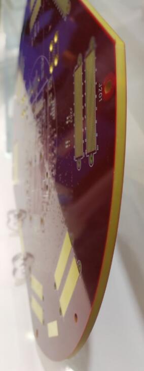
1.As an important electronic connector, PCB is used for almost all electronic products, is considered “the mother of electronic system products,” its technological changes and market trends have become the focus of attention of many businesses.
Currently, there are two obvious trends in electronic products: one is thin and short,the other is high frequency,high speed drive downstream PCB accordingly to high density, high integration, encapsulation, subtle, and the direction of multiple stratification, growing demand for the top layer PCB and the HDI.
Top pcb board wiring length is short, low impedance circuit, high-frequency high-speed work, stable performance, can take on more complex function, is to the high frequency electronic technology, multi-function large capacity development inevitable trend.In particular, the in-depth application of large-scale integrated circuits will further drive PCB to high precision and high level.
2.At present, PCB is mainly used for household appliances, PC, desktop and other electronic products, while high-end applications such as high performance multi-way servers and aerospace are required to have more than 10 layers of PCB.Take the server as an example, the PCB board on the single and two-way server is generally between 4-8 layers, while the main board of the high-end server, such as 4 and 8 roads, requires more than 16 layers, and the backplate requirement is above 20 layers.
HDI wiring density relative to ordinary multilayer pcb board has obvious advantages,which is the main choice of mainboard of current smartphone.Smartphone function increasingly complex and volume to lightweight development, less and less space for the main board, require limited carrying more of the components on the main board,ordinary multi-layer board has been difficult to meet the demand.
High-density interconnection circuit board (HDI) adopts the laminated legal system board, the ordinary multilayer board as the core board stacking, the use of drilling, and hole metallization process, making all layers of the line between the internal connection function. Compared with conventional through-hole only multilayer pcb boards, HDI accurately sets the number of blind vias and buried vias to reduce the number of vias, saves PCB layout area, and significantly increases component density, thus rapidly completing the multi-layer operation in smartphones Laminating alternatives.
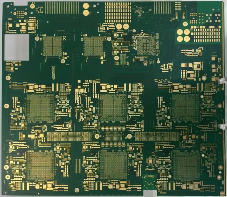
The technical difference of HDI is reflected in the increment stacked number, the more layer quantity, the more difficult the technology.HDI can be divided into single stacked HDI, doule stacked HDI, triple stacked HDI,or high stacked HDI, etc., the number of layers is expressed as C+N+ C, where N is the number of normal core laminar, and C is the number of added layers, namely the stacked number of HDI..High stacked HDI cabling has higher density, but at the same time, it has more pressure, such as position, punch hole and copper plating, etc., which has higher requirements on the technical process and process capability of the manufacturer.
Popular in recent years in the high-end smartphone arbitrary layer HDI is the highest stacked of HDI, require any have blind holes connection between adjacent layers, on the basis of ordinary HDI would save nearly half of the volume, so as to make more room for battery and other parts.
Any layer of HDI requires the use of advanced technologies such as laser drilling and electroplated hole plugs, which is the most difficult production and the highest value-added HDI type, which can best reflect the technical level of HDI.
Two important trends of the automobile industry are intelligent and electric.ADAS (Advanced Driver Assistance System) as the transition of complete intelligent driving before, has become a major automakers and crossover of Internet giant rushed to the layout of the new strategic highland, it involves the electronic device cover nearly all of the whole vehicle driving and safety related System, with the rapid penetration of ADAS, comprehensive automobile electronic level will be raised.
3.And new energy vehicles is representing the direction of the electric car, compared with the traditional car, the higher request of electronic level, electronic devices in traditional limousine costs accounted for about 25%, 45% to 45% in the new energy vehicles, unique power control system (BMS,VCU and MCU),makes the vehicle PCB usage is larger than the traditional car, the three power control system PCB usage average of about 3-5 square meters, the amount of vehicle PCB Between 5-8 square meters.
4.The growth of ADAS and new energy vehicles, driven by two wheels, has also kept the automotive electronics market growing at an annual rate of more than 15 percent in recent years.Accordingly, the market of PCB will continue upward, and it is predicted that the production of PCB will exceed $4 billion in 2018, and the growth trend is very clear,injecting new momentum into the PCB industry.
5.Smartphones have been a major driver of the PCB industry in the past.Mobile Internet era, more and more users from PC to mobile terminal equipment, the status of the PC computing platform quickly replaced by the mobile terminal, since 2008, global consumer electronic components enterprise fast development, especially in 2012 ~ 2014, smartphone into rapid infiltration.Therefore, the rapid growth of PCB is driven by the downstream of mobile terminals represented by smart phones.Between 2010 and 2014, the smartphone market in the downstream of PCB reached an average annual compound growth rate of 24%, far exceeding that of other downstream industries, providing the main growth drivers for the PCB industry.
In high-end PCB, HDI, for example, mobile phone is a traditional HDI market, in 2015, for example, smartphones accounted for more than half the proportion, and from the perspective of smart phones, the present new works almost all products using HDI as motherboard.
Both from the perspective of PCB and high-end HDI, it is the high speed of smartphone growth that leads to the prosperity demand downstream, thus supporting the growth of global PCB advantage enterprises.
But there is no denying that the smartphone market has slowed down since 2014, after a rapid infiltration period and the gradual entry of smartphones into the stock era.On the global market, the latest forecast from IDC2016 released in November 2016, the global smartphone shipments in 2016 are expected to be 1.45 billion, with a significant jump in growth of just 0.6 percent.In terms of growth data, although half of PCB’s downstream applications are still supported by mobile phones, most PCB categories, including HDI, have slowed in the mobile terminal area.
Although in the context of the economic downturn, smartphone industry into the second half is a foregone conclusion, but on the basis of the large stock, due to the demonstration effect other vendors to follow up, consumer demand will drive the replacement.The big stock market of smart phones still has huge potential, and the vendors of the terminals will do their best to improve consumers’ pain points so as to stimulate demand and grab market share.As a result, the smart phone, as the main downstream application of PCB in the past, has great potential for the growth of PCB in the huge stock boundary.
Over the past two or three years of smart phone development trend, fingerprint recognition, 3D Touch, big screen, dual camera and other continuous innovation has been emerging, but also continue to stimulate replacement upgrade.
In the context of mobile phones entering the age of stock, the large volume basis determines that the relative growth caused by the innovation of selling points will still lead to a huge increase in the absolute quantity of demand.Stock of innovation also affects global PCB, if future smartphone innovation upgrade in PCB, considering the existing mobile phone manufacturer urgent shipment size and other follow-up will, innovation upgrade will accelerate penetration, thus appeared similar to the optical, acoustic, etc.
6.Focusing on the PCB industry, the outbreak of FPC and any layer of interconnection HDI attracts other manufacturers to follow up, and the point radiates to the surface to form a model of rapid penetration:
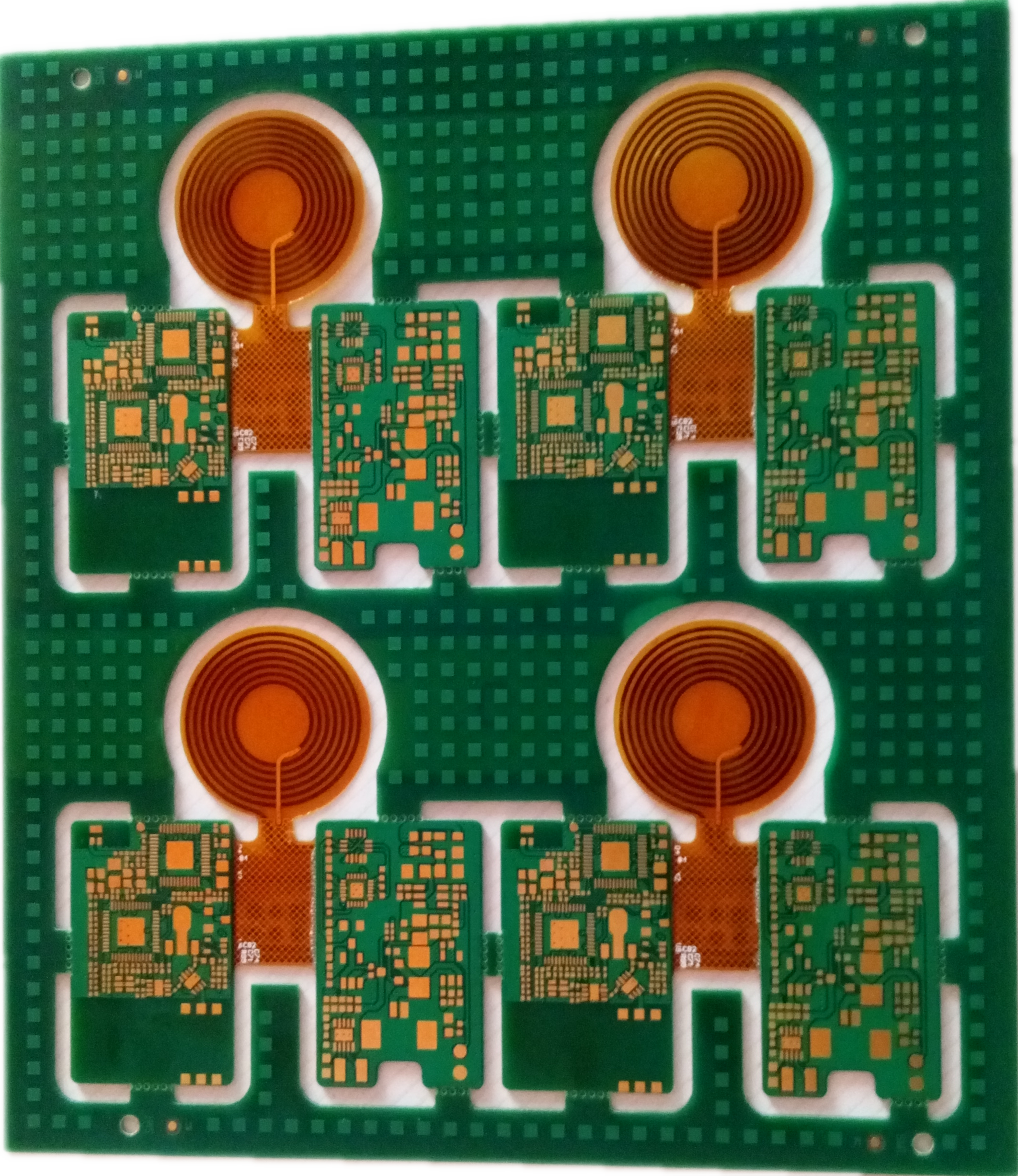
FPC is also known as “flexible pcb”,is a flexible polyimide or polyester film base material made of a flexible printed circuit board, with the high density of wiring, light weight, thickness thin, flexible, high flexibility, catering to the trend of the electronic product lightweight, flexible trend.
Used in its iPhone up to 16 pieces of FPC, procurement is the world’s largest FPC, world’s top six FPC manufacturer’s main customers are manufacturers such as apple, samsung, huawei, OPPO under apple demonstration also enhance its FPC usage of smartphones.
Smartphones as the primary driving force, the growth of FPC is benefit from apple and its demonstration effect, FPC rapidly permeate, 09 can maintain high growth, every year since 15 years as the only bright spot in PCB industry, became the only positive growth category.
7.Substrate-Like PCB (referred to as SLP) in the HDI technology, based on the M-SAP process, can further refine the line, is a new generation of fine line printed circuit board.
The class board (SLP) is the next generation PCB hardboard, which can be shortened from 40/40 microns of HDI to 30/30 microns.From process point of view, class loading board closer to used in the semiconductor packaging IC board, but has yet to reach the IC of the specifications of the load board, and its purpose is still carrying all sorts of passive components, the main result is still belongs to the category of the PCB.For this new fine line printing plate category, we will interpret the three dimensions of its import background, manufacturing process and potential suppliers.Why do you want to import class load board: extremely refined line superposition SIP packaging requirements, high density is still the main line, smart phones, tablets, and wearable devices and other electronic products to develop in the direction of miniaturization and muti_function change, to carry on the number of components is greatly increased for circuit board space, however, more and more limited.
In this context, PCB wire width, spacing, the diameter of the micro panel and the hole center distance, and the conductor layer and the thickness of insulating layer are falling, which make the PCB to reduce size, weight and volume of cases, it can accommodate more components.As Moore’s law is to semiconductors, high density is a persistent pursuit of printed circuit boards:
Extremely detailed circuit requirements are higher than HDI.High density drives the PCB to refine the line, and the pitch of the ball (BGA) is shortened.
In a few years ago, the 0.6 mm to 0.8 mm pitch technology has been used in the handheld devices, this generation of smart phones, because the quantity of I/O component and product miniaturization, PCB widely USES the technology of 0.4 mm pitch.This trend is developing towards 0.3mm. In fact, the development of 0.3mm gap technology for mobile terminals has already begun.At the same time, the size of the micropore and the diameter of the connecting disc have been reduced to 75 mm and 200 mm respectively.
The industry’s goal is to drop micropores and discs to 50mm and 150mm respectively in the next few years.The 0.3mm spacing design specification requires that the line width line is 30/30μm.
he class board fits the SIP packaging specification more.SIP system level packaging technology, based on the definition of international semiconductor line organization (ITRS) : SIP for multiple active electronic components with different functions and optional passive components, and other devices such as MEMS or optical device priority together, to achieve a certain function of a single standard packaging, packaging technology to form a system or subsystem.
There are usually two ways to realize the function of electronic system, one is SOC, and the electronic system is realized on the single chip with high integration.Another is SIP, which integrates CMOS and other integrated circuits and electronic components into a package using mature combination or interconnection technology, which can achieve the whole machine function through the parallel overlay of various functional chips.
The class board belongs to PCB hardboard, and its process is between high order HDI and IC plate, and the high-end HDI manufacturers and IC board manufacturers have the opportunity to participate.
HDI manufacturers are more dynamic, yield will be key.Compared with IC plate, HDI has become increasingly competitive and has become a red sea market, with profit margins declining.Face the class loading board, the opportunity of HDI manufacturers can to get the new orders, on one hand, on the other hand can realize product upgrade, optimizing the product mix and the level of earnings, therefore intend to stronger, more powerful the first layout.
Due to the process higher class loading board, HDI manufacturers to invest or new manufacturing equipment modification, and MSAP process technology for HDI manufacturers also requires learning time, from the subtraction method into MSAP, product yield will be key.
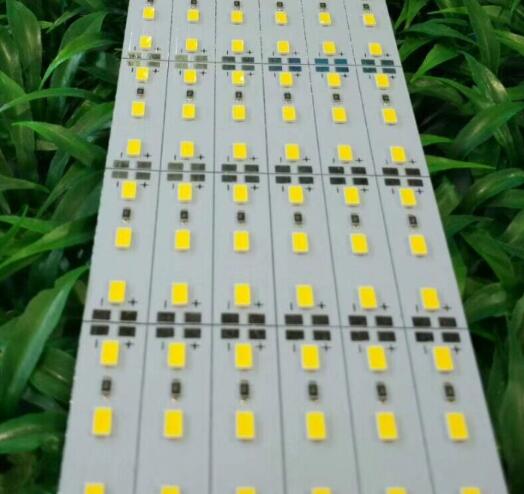
8.LED rapid development of high thermal conductivity CCL become a hot spot.The small spacing LED has the advantages of unspelt, good display effect and long service life. In recent years, it has begun to permeate, and it has been growing rapidly. Accordingly, the required high thermal conductivity CCL has become a hot spot.
Vehicle PCB on the product quality and reliability requirements are very strict, and more use of special performance materials CCL.Automotive electronics is an important PCB downstream applications. Automotive electronic products must first meet the automotive as a means of transport must have the characteristics of temperature, climate, voltage fluctuations, electromagnetic interference, vibration and other adaptive ability to higher requirements for automotive PCB materials put forward higher requirements, the use of more Special performance materials (such as high Tg materials, anti-CAF (compressed asbestos fiber) materials, thick copper materials and ceramic materials, etc.) CCL.


