Welcome to KingSong PCB Technology
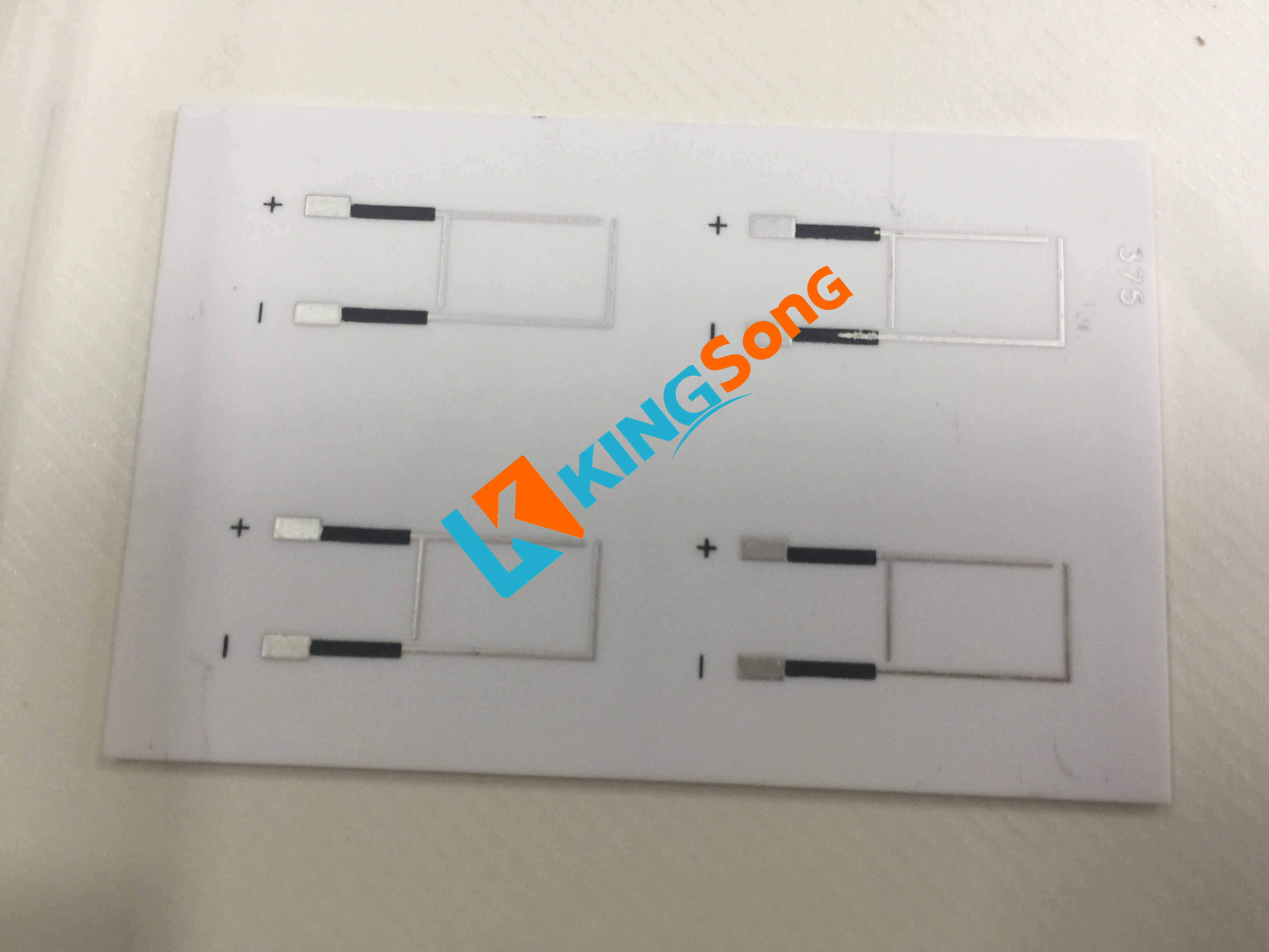
Image:Ceramic Antenna PCB Prototype Manufacturing Process

1.Ceramic PCB Board Capabilities:
Layer:1,2
Material:96% Alumina,99% Aluminium nitride(AIN),Sapphire,High Borosilicate Glass
Material Thickness(mm):0.38,0.635,0.5,1.0,1.2,1.5
Material Size(mm):120*120,127*127,132*132,140*130,190*140
Min Hole:0.075mm
Min Line width/space:0.1/0.1mm
Laser Outline: line width:0.1mm,tolerance:+/-0.1mm
Surface Finish:Immersion Silver,Immersion Gold,Immersion Tin,OSP
Copper Thickness(oz):H/H 1/1 2/2 3/3 4/4 5/5 6/6 7/7 8/8 9/9 10/10
Thermal conductivity value: 20~27W/m.K for Alumina; 180W~220W/m.K for Aluminium nitride , 27~30W/m.K for Sapphire,2 ~ 5 W/m.K for High Borosilicate Glass
Product Description:
Ceramic Antenna PCB Prototype is a high thermal conductivity substrate composed of high-conductivity dielectric Ceramic Antenna PCB Prototype composed of noble metal and high thermal conductivity insulating material,Can effectively solve the problem of low thermal conductivity PCB and aluminum substrate. To effectively heat the heat generated by high-temperature electronic components, increase component stability and extend the service life.
Ceramic PCB Features:
Do not need to change the original processing procedures
Excellent mechanical strength
With good thermal conductivity
With resistance to erosion
Good surface characteristics, excellent flatness and flatness
Good thermal shock resistance
Low curl degree
Good stability under high temperature can be processed into a variety of complex shapes
Ceramic PCB Application:
high-accuracy clock oscillator,
voltage controlled oscillator (VCXO),
temperature compensated crystal oscillators (TCXOs),
oven controlled crystal oscillators (OCXOs);
emiconductor cooler;
electric power electronic control module;
high insulation & high pressure device;
high temperature (up to 800C)
high power LED
High Power semiconductor modules
solid state relay (SSR)
DC-DC module power sources
electric power transmitter modules
Solar-panel arrays
Intelligent power devices
Automotive electronics
High power semiconductor module
Solar panel components
Lighting industry
Aerospace
Communications
The power electronics industry
2.Delivery time:
Sample:3-5 or 12-15 working days,
Mass production:5-7 or 12-15 working days
3.Package:Inner vacuum packing,Outer standard carton box packing.
4.Shipping:
A:By DHL,UPS,Fedex,TNT etc.
B:By sea for mass quantity according to customer’s requirement.
5.If need quotation for your PCB projects,pls provide following info:
A:Quote quantity,
B:Gerber file in 274-x format,
C:Technical requirement or parameters(material,layer,copper thickness,
board thickness,surface finishing,solder mask/silkscreen color…)
If any inquiry or want to learn more,please send email to us freely or chat by online system,thanks for your support in advance!