PCB circuit board interconnection method: plug connection method
In complex instruments and equipment, we often use the plug connection method. This “building block” structure not only ensure the quality of mass production products, reducing the cost of the system, and for debugging, maintenance provides a convenience. When the pcb equipment fail/brokens, the service people do not have to check the components(ie, check the cause of the failure, source to the specific components, that will takes a lot of time), just to determine which board is innormal and then you can immediately to replace it, time to solve the problem in the shortest possible , shorten the downtime, improve the utilization of equipment. The replaced circuit board can be carried out in ample time for repair, after repair as a spare part.
1. Printed Circuit Board Socket.
With complex instruments and equipments, we often use this connection way, this method is to make socket from the edge of PCB, the part of socket will manufactured as the size, connection points number, connection distance, marking points to design the layout, finally make PCB can be matched with special PCB Socket.
In the process of manufacture, the part of socket need pated gold surface finish, improve wear resistance, reduce contact resistance. This methos is easy to assemble, and the interchangeability and repair performance is good, is suitable for standardized PCB mass production . The short of this method is the improvement of the cost of printed circuit, has high requirements on printed circuit board manufacturing accuary, often due to poor contact of socket because of the osidation orreed aging. In order to improve the reliability of external connections, we often paralel lead the same lead circuit at the same time lead the connection points on the same or bith sides of PCB.
PCB Socket Connection method often used in muiti-boards structure products, socket with printed circuit board or bottom/floor board has Spring type and plug-in pin type.
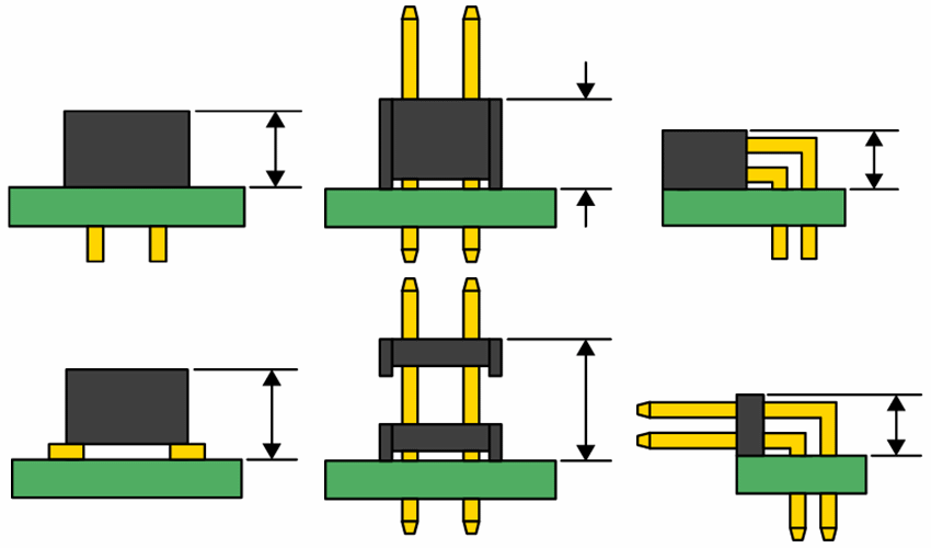
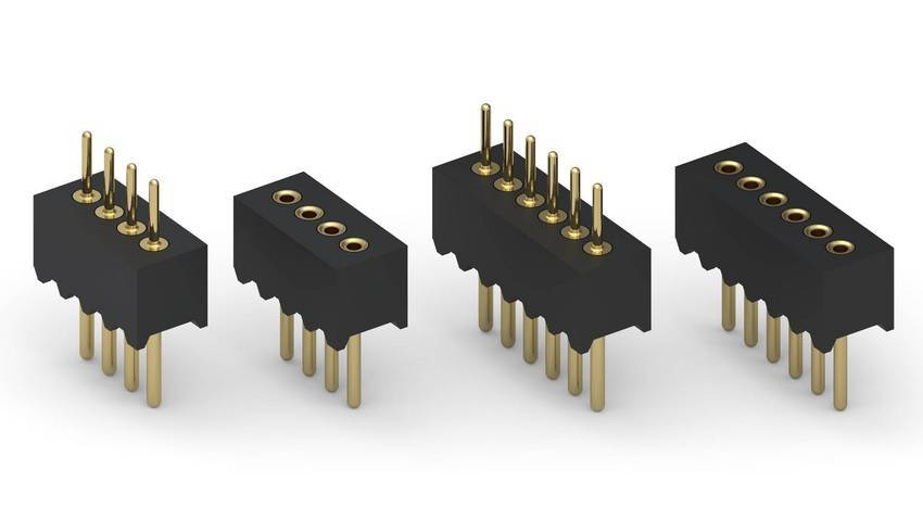
2. Standard Pin Connection
This method can be used for the external connection of printed circuit boards, expecially in small instruments. Through standard pin to connect two pinted circuit board, these 2 printed circuit boards usually parallel or vertial, it is easy to achiee mass production.


